
Laboratory of materials characterisation and processing in 3D and 4D

The Laboratory of materials characterisation and processing in 3D and 4D is located at IMDEA Materials Institute and is organised into three fundamental units:
- Electron Microscopy Unit
- X-ray Tomography Unit
- Additive Manufacturing Unit
The laboratory’s Scientific Manager is Dr. Juan Pedro Fernández. Each of the units also has the scientific supervision of the senior researchers responsible for each of the research lines.
Types of tests:
- SEM and TEM microstructural characterisation of materiales
- In situ deformation tests in SEM and TEM
- Structural and defect characterization by XCT
- Additive manufacturing of metal parts
Types of materials:
- Composites and nanocomposites
- Polymers
- Metal alloys
- Metal powder
The Laboratory of materials characterisation and processing in 3D and 4D is structured as follows:
Scientific Manager: Dr. Juan Pedro Fernández.
- Electron Microscopy Unit:
Scientific Advisor: Dr. Jon Molina.
Technical Staff: Dr. Manuel Avella, and Jesús Carreras.
- X-ray Tomography Unit:
Scientific Advisor: Dr. Federico Sket.
Technical Staff: Dr. Javier García.
- Additive Manufacturing Unit:
Scientific Advisor: Dr. Teresa Pérez Prado.
Technical Staff: Amalia San Román.
- Electron Microscopy Unit:
- Microstructure characterisation via controlled pressure scanning microscopy (SEM).
- Characterisation of deformation and fracture mechanisms through in-situ tests using controlled pressure scanning microscopy (SEM), and mechanical testing machines in metallic and composite materials.
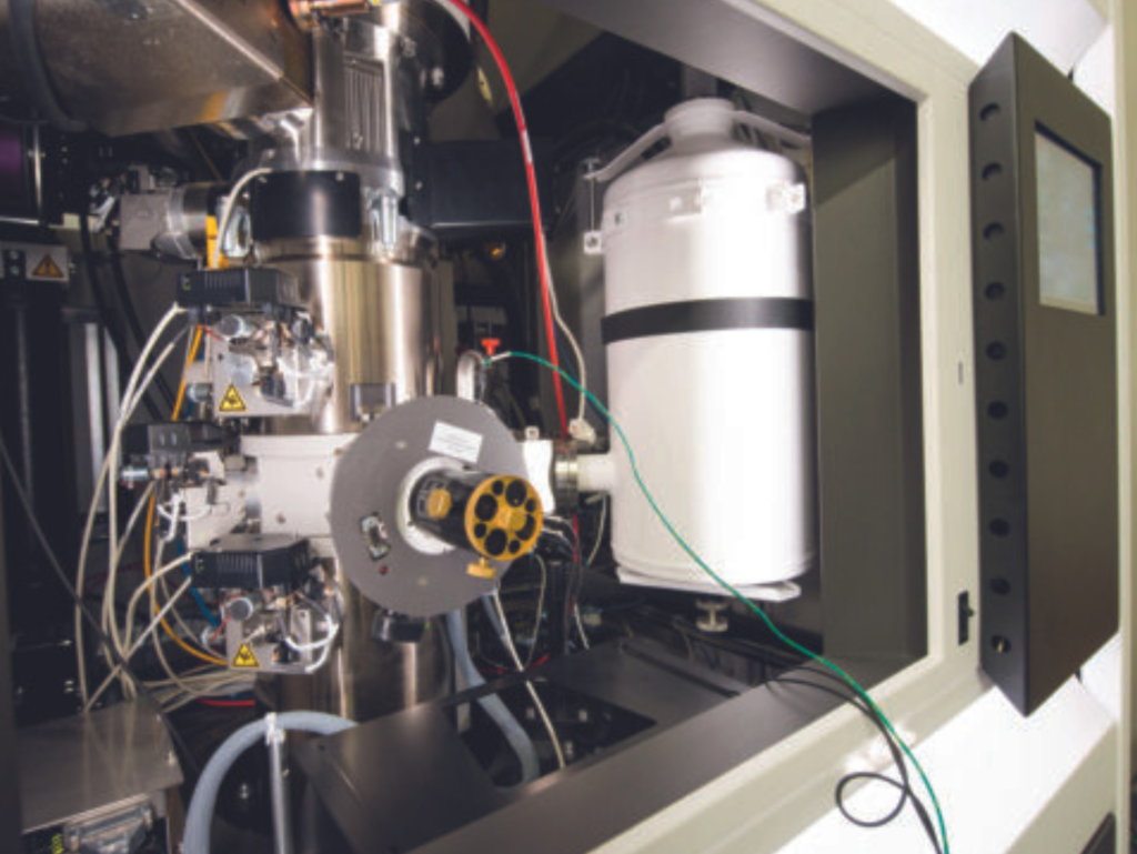
- Characterisation in TEM or STEM mode and chemical analysis performance in EDS; TEM, STEM and EDS mode tomography; in-situ mechanical tests inside the TEM using the Hysitron PIcoindenter PI95 holder.
- Processing of images obtained via electron microscopy.
- X-ray Tomography Unit:
- Characterisation of defects and internal structure by X-ray computed tomography.
- Characterisation of fracture mechanism via in-situ tests using X-ray computed tomography and mechanical testing.
- Processing of volumes obtained via X-ray tomography.
- Additive Manufacturing Unit
- Laser Powder Bed Fusión (LPBF) of metallic alloy samples.
Currently available equipment:
- Electron Microscopy Unit
- Thermofisher Scientific Apreo 2S LoVac FEG SEM microscope, equipped with a NiCol electron column with immersion lens and beam deceleration capabilities. Everhart-Thornley Detector (ETD), in-lens Trinity Detector System (T1,T2,T3), retractable backscatter detector (CBS/ABS), low-vacuum detector (LVD) and GAD-CBS/ABS for low vacuum mode.
- For more information on external use of the Thermofisher Apreo 2S SEM microscope, click here.
- FEI Talos F200X, FEG S/TEM microscope, which integrates a chemical analysis system by energy dispersive spectrometry (EDS), a CMOS digital camera to acquire images with a maximum resolution of 4×4 k, a tomography system to perform tomographies in TEM, STEM and EDS mode and a Hysitron PicoIndenter PI95 holder, to conduct in-situ nano-mechanical tests (S/TEM-Ind).
- For more information on external use of the Talos F200X TEM microscope, click here.
- Kammrath & Weiss in situ mechanical testing platform (tensile compression module), which enables tensile, compression, and 3- and 4-point bending tests on macroscopic specimens within the Thermo Fisher Scientific Apreo 2S LoVac FEG SEM, while simultaneously observing the surface using secondary electron, backscattered electron, EDS, and EBSD detectors. The equipment accommodates sub-standard specimens 30–60 mm in length, up to 10 mm in width, and 4 mm in thickness.
- For more information on external use of the Kammrath & Weiss in situ mechanical testing platform , click here.
- Alemnis Nanoindenter for in situ micro/nano-mechanical testing, which enables nanoindentation testing to measure mechanical properties such as hardness and elastic modulus, as well as micropillar compression testing to determine stress-strain curves at the micro scale. The system allows for video recording during testing to study deformation mechanisms, as well as testing at high temperatures (up to 1000 °C) and low temperatures (down to -150 °C).
- For more information on external use of the Alemnis Nanoindenter for in situ micro/nano-mechanical testing, click here.
- X-ray Tomography Unit
- GE (Phoenix) Nanotom 160 kV with a Hamamatsu 7942-25SK detector (2K x 2K) and tungsten and molybdenum targets, with a nanofocus X-ray source. This equipment is capable of both radiography (RX) and computed tomography (XCT) modes.
- For more information on external use of the Phoenix Nanotom X-ray tomograph, click here.
- Zeiss Xradia 620 Versa tomograph with flat panel detector (3k × 2k pixels) and CCD camera (2k × 2k pixels) with the possibility of different objectives (0.4X, 4X, 20X, and 40X). The equipment features a focused X-ray tube with a tungsten emitter and voltage up to 160 kV. This equipment allows for the acquisition of radiographs (RX) and computed tomography (XCT), as well as the possibility of performing diffraction tomography (DCT), which can determine the size and orientation of grains in metallic materials.
- For more information on external use of the Zeiss Xradia 620 Versa tomograph, click here.
- Additive Manufacturing Unit
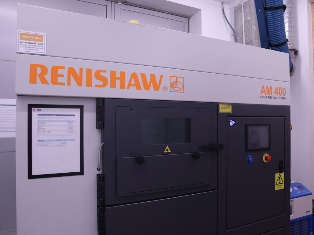
Renishaw AM400 Laser Powder Bed Fusion (LPBF) system for the additive manufacturing of metallic materials (Inconel, Aluminum, High entropy alloys, Nitinol, Nickel) with the following specifications:
- Laser power: 400 W
- Laser thickness: 20 to 100 micrometres
- Spot size: 70 micrometres
- Speed scanning: up to 2 m/s
- Build volume: 248 mm x 248 mm x 285 mm.
- Reduced build volume option available: 55mm x 78 mm x 78 mm
- For more information on external use of the Renishaw AM400 LPBF System, click here.
For further information about current rates for Thermofisher Apreo 2S SEM microscope services, click here.
For further information and current rates for Talos F200X TEM microscope services, click here.
For further information and current rates for Kammrath & Weiss in situ mechanical testing platform services, click here.
For further information and current rates for Alemnis Nanoindenter for in situ micro/nano-mechanical testing services, click here.
For further information and current rates for Phoenix Nanotom X-ray tomography services, click here.
For further information and current rates for Zeiss Xradia 620 Versa tomography services, click here.
For further information and current rates for the Renishaw AM400 LPBF Additive Manufacturing System, click here.
The rates for the rest of the services will vary depending on the characterization work required (type of material, type of tests, number of samples, test standards, etc.).
Location
IMDEA Materials Institute
C/ Eric Kandel, 2
Tecnogetafe
28906, Getafe, Madrid (España)
Telephone: (+34) 91 549 34 22
Equipment

Grants received
The Laboratory of Materials Characterisation and Processing in 3D and 4D (REDLAB-016) has received funding from the Community of Madrid and the European Union through the European Regional Development Fund (ERDF) under action reference 2024-REDLAB/ TEC-33811 for the acquisition of scientific and technical equipment through the call for Grants for the acquisition of scientific and technical equipment for laboratories in the network of laboratories and scientific and technical infrastructures of the Community of Madrid (REDLAB), which approves the call for 2024, co-financed by the European Regional Development Fund.